Key learning points
- PCBs are manufactured using CNC machining or chemical etching
- CNC machining mills away copper using a CNC router and design software
- chemical etching uses UV light, photo-resist, and chemicals to remove copper
- CNC machining is safer and less wasteful, but slower
- chemical etching is faster and cheaper, but uses hazardous chemicals
- PCB design involves placing components, creating tracks and pads, and using design software
- PCB amendment involves updating components, modifying tracks, and repositioning pads
- PCBs are used for space-saving, reliable connections, ease of repair, and professional appearance
Manufacturing printed circuit boards (PCBs)
There are two main ways to manufacture printed circuit boards (PCBs):
- CNC machining
- Chemical etching
PCB manufacture using CNC machining
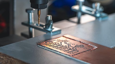
Using a CNC milling machine to mill away the unwanted copper to create a circuit board
Tools required: Computer with PCB design software, CNC router and copper-clad board
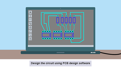
Image caption, Design
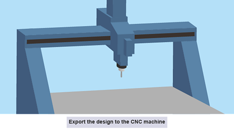
Image caption, Export to CNC
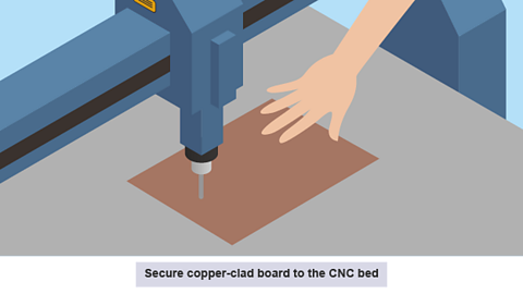
Image caption, Secure
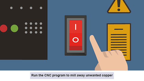
Image caption, Mill
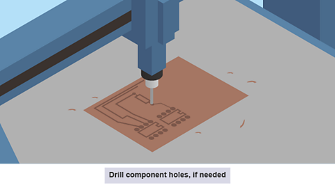
Image caption, Drill
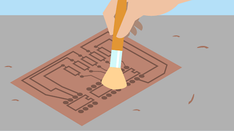
Image caption, Clean
1 of 6
Process:
- Design the circuit using PCB design software
- Export the design to the CNC machine.
- Secure copper-clad board to the CNC bed.
- Run the CNC program to mill away unwanted copper.
- Drill component holes, if needed.
- Clean the board to remove debris.
- Pros: safer, no chemicals, less waste
- Cons: slower for complex designs
PCB manufacture using chemical etching
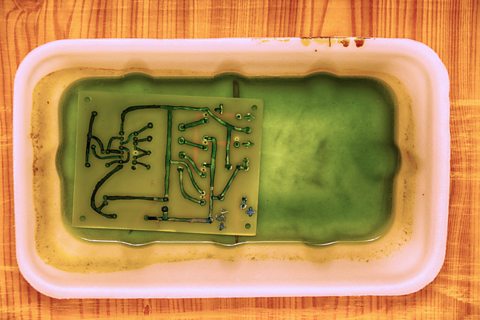
Using a chemical method to remove the unwanted copper to create a circuit board.
Tools required: UV light box, photo-resist board, developer solution and an etching tank.
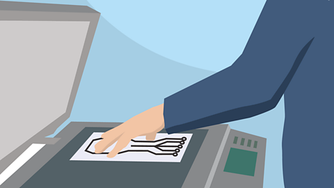
Image caption, Copy
Photocopy or trace a copy of the circuit onto an acetate sheet to make a mask of the circuit. This is called the PCB Artwork.
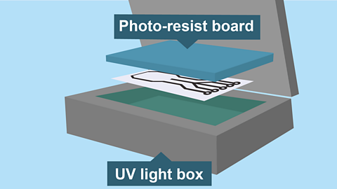
Image caption, Expose
Place the mask into an ultra-violet light box and set the photo-resist board on top. Close the box and expose for three minutes.
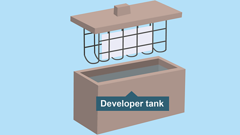
Image caption, Develop
Place the board carefully into the developing solution (Sodium Hydroxide) to remove all the film except where the tracks are. Once you can see the copper tracks rinse under water.
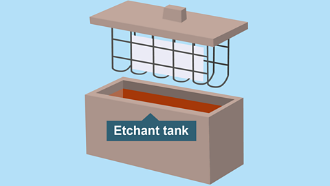
Image caption, Etch
The chemical (Ferric Chloride) is heated to about 50°C. It will dissolve any unprotected copper leaving a PCB with copper tracks on one side.
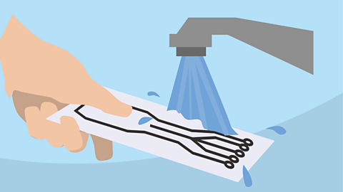
Image caption, Rinse
Rinse with water.
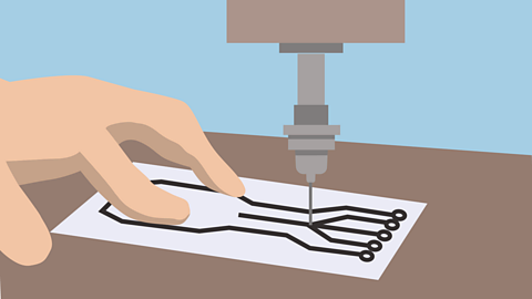
Image caption, Drill
The last stage is drilling the holes for the components. A small PCB drill is used for this purpose.
1 of 6
Process:
- Design the circuit using PCB design software. Print the design onto a transparency/acetate sheet. This is called the PCB artwork
- Prepare the photo-resist board by peeling off the protective film. Place the transparency on the photo-resist board. Expose to UV light in a light box (approx 3 minutes)
- Develop the board in Sodium Hydroxide solution (about 10 seconds). Rinse the board with clean water
- Place in a heated etching tank of Ferric Chloride (15-45 minutes). This will remove unwanted copper. Remove and rinse when etching is complete.
- Drill component holes with a PCB drill
- Pros: faster for multiple boards, cheaper
- Cons: uses harsh chemicals, more environmental concerns
Why use PCBs?
- space-saving compared to just using components soldered using loose wires
- easier to repair - just swap components
- more reliable connections
- professional appearance
Electrical safety in circuit production
When working with printed circuit boards (PCBs) or breadboardA breadboard is a plastic board with a grid of holes that allow you to connect electronic components without soldering. Useful when prototyping circuits., it's crucial to stay safe. Here are the key hazards to watch out for:
short circuits:
- double-check connections before powering on
- use insulated tools to avoid accidental shorts
- keep metal objects (like paperclips) away from live circuits
component damage:
- handle components gently, especially integrated circuits (IC)
- be aware of static electricity
- check polarity of capacitors and diodes before inserting
burns:
- let soldering irons cool completely before storing
- be careful with hot components after extended use
chemical exposure (for pcb etching):
- wear gloves and eye protection
- work in a well-ventilated area
- dispose of chemicals properly
Tidy workspace = safer workspace.
Keep things organised and you'll reduce risks!
Test yourself
More on Electronic control systems
Find out more by working through a topic
- count3 of 8
- count5 of 8
- count6 of 8
